Atomic Layer Deposition (ALD) Equipment Market Size & Growth Forecast 2027–2036, By Segments (Deposition Method, Application, Equipment, Film Type), Regional Demand Trends (North America, Asia Pacific, Europe), Key Country Insights (U.S., Japan, South Korea, Germany, France, Italy), and Competitive Landscape
Market Size and Growoth Outlook
ALD Equipment Market size stood at USD 5.04 Billion in 2026 and is predicted to grow at 11.34% CAGR from 2027 to 2036, exceeding USD 14.76 Billion by 2036. The industry revenue for 2027 is calculated at USD 5.53 Billion.
Get more details on this report
Request Free Sample ReportAtomic Layer Deposition (ALD) Equipment Market Intelligence Snapshot
Regional Market Dynamics
- North America leads due to advanced semiconductor manufacturing, demand for miniaturized components, and investment in next-generation fabrication technologies and advanced electronics.
- Continued R&D in memory, logic devices, and emerging semiconductor applications is supporting demand for precise thin-film deposition and sustaining regional growth.
Segment Momentum
- Spatial ALD captured 36.83% of the market in 2026 because it delivers high-throughput, precise, and uniform thin-film deposition, making it well suited for high-volume semiconductor and advanced electronics manufacturing.
- The energy & power segment is projected to grow the fastest as advanced thin-film technologies gain wider use in energy storage, power electronics, and next-generation energy devices requiring reliable deposition solutions.
Market Expansion Drivers
- Advanced semiconductor node scaling driving need for ultra-precise thin-film deposition systems
- Expansion of 3D NAND and DRAM manufacturing increasing multilayer deposition requirements
- Growing use of high-k dielectrics and wide-bandgap semiconductors boosting ALD adoption
Leading Market Participants
- Key companies in the ALD equipment market include ASM International N.V. (Netherlands), Applied Materials Inc. (United States), Lam Research Corporation (United States), Tokyo Electron Limited (Japan), Veeco Instruments Inc. (United States), Aixtron SE (Germany), Oxford Instruments plc (United Kingdom), Beneq Oy (Finland), CVD Equipment Corporation (United States), Hitachi High-Technologies Corporation (Japan)
Global Market Forecast Snapshot
Market Outlook
- 2026 Market Size: USD 5.04 Billion
- 2027 Estimated Market Size: USD 5.53 Billion
- Projected Market Size: USD 14.76 Billion by 2036
- Growth Forecast: 11.34% CAGR (2027-2036)
Regional and Segment Outlook
- Leading Regional Market: North America
- High-Growth Regional Hub: North America
- Core Revenue Segment: Spatial ALD (Deposition Method) | Computing Sector (Application) | Single-wafer Reactors (Equipment) | Oxide Film (Film Type)
- Emerging Opportunity Segment: Plasma Enhanced ALD (Deposition Method) | Energy & Power (Application) | Spatial ALD Reactors (Equipment) | Metal Film (Film Type)
Market Growth Drivers and Industry Trends
Advanced semiconductor node scaling driving need for ultra-precise thin-film deposition systems
The transition toward smaller semiconductor geometries and increasingly complex chip architectures is creating demand for highly controlled deposition processes, which will drive the ALD equipment market growth. Advanced nodes require atomic-level thickness management and exceptional film uniformity to maintain device performance, power efficiency, and reliability as transistor dimensions continue to shrink. Atomic layer deposition enables precise material layering through sequential surface reactions, making it essential for manufacturing advanced logic devices and other high-performance semiconductor components where conventional deposition methods face limitations.
Expansion of 3D NAND and DRAM manufacturing increasing multilayer deposition requirements
The ALD equipment market growth is driven by the rapid expansion of memory semiconductor production, where increasing layer counts in 3D NAND and evolving DRAM designs require advanced deposition capabilities. Manufacturers are adopting atomic layer deposition technologies to achieve conformal coatings across intricate three-dimensional structures, ensuring consistent electrical characteristics throughout multilayer architectures. The growing complexity of memory devices is increasing the need for reliable thin-film processes that support higher storage density, improved performance, and enhanced manufacturing precision.
Growing use of high-k dielectrics and wide-bandgap semiconductors boosting ALD adoption
Rising adoption of advanced materials such as high-k dielectrics and wide-bandgap semiconductors will propel the ALD equipment market growth by expanding applications beyond traditional semiconductor fabrication. These materials require precise deposition techniques to achieve desired electrical properties, thermal stability, and device efficiency in applications including advanced processors, power electronics, and next-generation semiconductor systems. ALD technology provides the controlled material integration needed for these emerging applications, supporting broader utilization across specialized semiconductor manufacturing processes.
| Growth Driver | Impact on CAGR | Regulatory Influence | Geographic Relevance | Adoption Rate | Impact Timeline |
|---|---|---|---|---|---|
| Advanced semiconductor node scaling driving need for ultra-precise thin-film deposition systems | 3.4% | High | Asia Pacific, North America | High | Near Term |
| Expansion of 3D NAND and DRAM manufacturing increasing multilayer deposition requirements | 3.2% | High | Asia Pacific | High | Mid Term |
| Growing use of high-k dielectrics and wide-bandgap semiconductors boosting ALD adoption | 2.9% | High | North America, Europe | High | Mid Term |
Unlock insights tailored to your business with our bespoke market research solutions.
Click to get your customized report now.
Regional Demand Dynamics
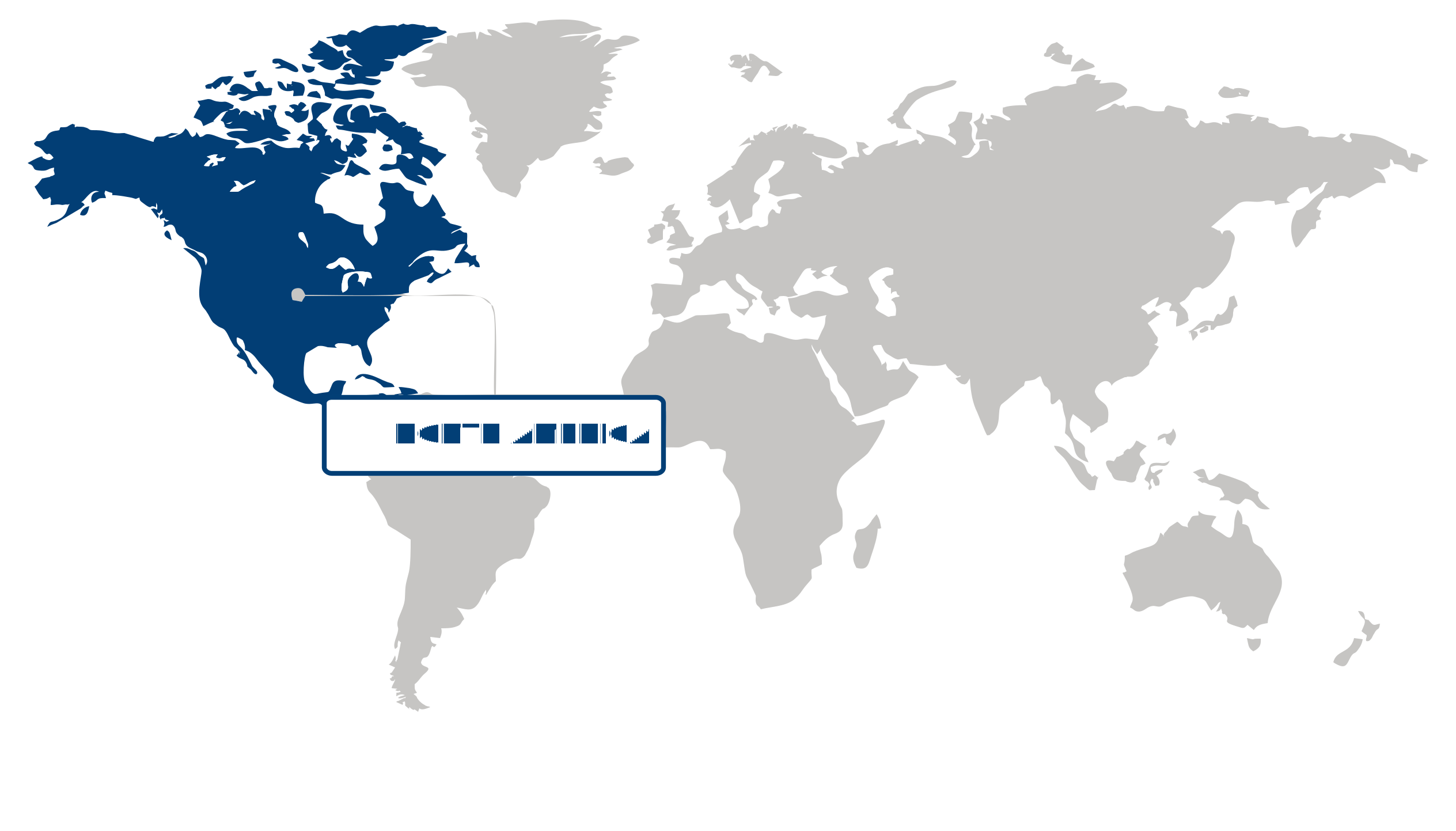
North America (Largest & Fastest-Growing Region)
North America led the atomic layer deposition (ALD) equipment market and is also expected to remain the fastest-growing region, supported by advanced semiconductor manufacturing capabilities, strong demand for miniaturized electronic components, and continued investment in next-generation fabrication technologies. The increasing complexity of semiconductor architectures is strengthening the need for highly precise thin-film deposition processes that can provide uniform material layers at extremely small dimensions. Expanding research and development in advanced electronics, memory, logic devices, and emerging semiconductor applications is further creating favorable conditions for ALD equipment adoption.
| Parameter | North America | Asia Pacific | Europe | Latin America | MEA |
|---|---|---|---|---|---|
| Innovation Hub i Scale Nascent Developing Advanced | |||||
| Cost-Sensitive Region i Scale Low Medium High | |||||
| Regulatory Environment i Scale Restrictive Neutral Supportive | |||||
| Demand Drivers i Scale Weak Moderate Strong | |||||
| Development Stage i Scale Emerging Developing Developed | |||||
| Adoption Rate i Scale Low Medium High | |||||
| New Entrants / Startups i Scale Sparse Moderate Dense | |||||
| Macro Indicators i Scale Weak Stable Strong |
Key Country Insights
United States 🇺🇸
Advanced Semiconductor FabricationThe U.S. continues investing in atomic layer deposition equipment to support advanced semiconductor manufacturing, specialty electronics, and research facilities. Demand is driven by precision deposition technologies capable of meeting increasingly complex chip fabrication requirements.
Germany 🇩🇪
Precision Manufacturing ApplicationsGermany utilizes atomic layer deposition equipment across semiconductor, optics, and advanced industrial manufacturing. Companies prioritize process consistency, high-quality thin-film performance, and equipment capable of supporting specialized production environments.
Japan 🇯🇵
Materials Innovation PlatformJapan advances atomic layer deposition equipment adoption through semiconductor materials development and precision electronics manufacturing. The market emphasizes highly controlled deposition processes that enable next-generation devices and advanced component miniaturization.
South Korea 🇰🇷
Chip Production EnhancementSouth Korea is expanding the deployment of atomic layer deposition equipment to support advanced memory and logic semiconductor manufacturing. Manufacturers are investing in high-throughput deposition systems that improve process precision for increasingly complex device architectures.
France 🇫🇷
Research-Driven Thin FilmsFrance applies atomic layer deposition equipment across semiconductor research, photonics, and advanced materials development. Organizations are emphasizing flexible deposition platforms that support innovation in precision thin-film applications.
Italy 🇮🇹
Advanced Electronics ManufacturingItaly is strengthening atomic layer deposition capabilities for microelectronics, industrial components, and research-driven manufacturing. Companies are focusing on precise thin-film deposition technologies that enhance product quality across specialized electronic applications.
Segment Leadership and Growth Trends
Go beyond the chart, access full insights & data tables
Request Free Sample ReportDeposition Method Segment Analysis: Spatial ALD (Largest Segment) vs Plasma Enhanced ALD (Fastest-Growing Segment)
The ALD equipment market was led by the spatial ALD segment, which captured 36.83% of the market share in 2026. Its leadership is supported by its ability to deliver higher throughput while maintaining precise and uniform thin-film deposition across large substrates. The technology is well suited for high-volume manufacturing environments where productivity and coating consistency are critical, making it a preferred choice for semiconductor and advanced electronics production. Continued demand for efficient deposition processes further reinforces its dominant market position.
Plasma enhanced ALD is the fastest-growing deposition method owing to its capability to achieve high-quality film deposition at lower process temperatures while improving material properties and process flexibility. Its expanding use in advanced semiconductor fabrication, next-generation electronic devices, and complex material applications is driving broader adoption. Increasing demand for high-performance thin films with superior conformality and enhanced process control continues to support the segment's growth.
Application Segment Analysis: Computing Sector (Largest Segment) vs Energy & Power (Fastest-Growing Segment)
The computing sector accounted for 35.86% of the market share in 2026, making it the largest application segment. Demand is driven by the continuous advancement of processors, memory devices, and high-performance computing hardware that require highly precise thin-film deposition technologies. Ongoing miniaturization of semiconductor components and increasing requirements for manufacturing accuracy continue to strengthen the computing sector's leading position within the market.
In the ALD equipment market, the energy & power segment is emerging as the fastest-growing application as advanced thin-film technologies gain wider adoption in energy storage systems, power electronics, and next-generation energy devices. Growing investments in energy efficiency, renewable energy technologies, and high-performance electronic components are increasing the need for reliable deposition solutions capable of improving device performance, durability, and operational efficiency.
Equipment Segment Analysis: Single-wafer Reactors (Largest Segment) vs Spatial ALD Reactors (Fastest-Growing Segment)
Single-wafer reactors held the largest position within the equipment segment due to their ability to deliver exceptional process precision, uniformity, and repeatability for advanced semiconductor manufacturing. Their suitability for producing complex device architectures and maintaining strict process control has made them a preferred solution for applications requiring consistent deposition quality and high manufacturing standards.
Spatial ALD reactors represent the fastest-growing equipment segment as manufacturers increasingly seek higher throughput and improved production efficiency without compromising deposition quality. Their capability to support continuous processing and large-scale manufacturing aligns with rising demand for advanced electronic components, making them an increasingly attractive choice for high-volume production environments.
| Segment | Sub-Segment | Largest Segment | Fastest Growing |
|---|---|---|---|
| Deposition Method | Plasma Enhanced ALD, Thermal ALD, Spatial ALD, Power ALD, Others | Spatial ALD | Plasma Enhanced ALD |
| Application | Computing Sector, Data Centers, Consumer Electronics, Healthcare and Biomedical, Automotive, Energy & Power | Computing Sector | Energy & Power |
| Equipment | Batch Reactors, Single-wafer Reactors, Spatial ALD Reactors, Remote Plasma ALD Reactors | Single-wafer Reactors | Spatial ALD Reactors |
| Film Type | Metal Film, Oxide Film, Sulfide Film, Nitride Film, Fluoride Film | Oxide Film | Metal Film |
Competitive Landscape and Market Positioning
Major players in the atomic layer deposition (ALD) equipment market:
- ASM International N.V. (Netherlands)
- Applied Materials, Inc. (United States)
- Lam Research Corporation (United States)
- Tokyo Electron Limited (Japan)
- Veeco Instruments, Inc. (United States)
- Aixtron SE (Germany)
- Oxford Instruments plc (United Kingdom)
- Beneq Oy (Finland)
- CVD Equipment Corporation (United States)
- Hitachi High-Technologies Corporation (Japan)
Technological precision has become the defining arena for competition as equipment developers seek to improve film uniformity, process repeatability, and compatibility with increasingly complex device architectures. Manufacturers are refining deposition platforms to support a broader range of advanced materials while reducing process variability and enhancing throughput for research and commercial production environments. As customer requirements become more application-specific, the ability to provide flexible process configurations, comprehensive technical support, and rapid process optimization is gaining importance alongside core equipment performance. Competitive momentum is therefore shifting toward organizations capable of translating materials expertise into scalable manufacturing solutions across multiple high-value applications.
| Company | Market Share | Company Revenue | Revenue CAGR (%) | Product Portfolio | Geographic Presence | Innovation / R&D Focus | Strategic Developments |
|---|---|---|---|---|---|---|---|
| ASM International N.V. (Netherlands) | |||||||
| Applied Materials Inc. (United States) | |||||||
| Lam Research Corporation (United States) | |||||||
| Tokyo Electron Limited (Japan) | |||||||
| Veeco Instruments Inc. (United States) | |||||||
| Aixtron SE (Germany) | |||||||
| Oxford Instruments plc (United Kingdom) | |||||||
| Beneq Oy (Finland) | |||||||
| CVD Equipment Corporation (United States) | |||||||
| Hitachi High-Technologies Corporation (Japan) |
Industry Development/News
| Company Name | Date | Key Development |
|---|---|---|
| Beneq Oy | Nov-25 | Beneq Oy introduced the Transmute ALD platform, a next-generation deposition system for high-volume manufacturing of wide-bandgap power electronics, RF devices, and micro-LEDs. By integrating plasma pretreatment, plasma-enhanced ALD, and thermal ALD in a single platform, the system strengthens high-throughput production while enabling precise atomic-scale interface control for advanced semiconductor applications. |
| Forge Nano Inc | Sep-25 | Forge Nano Inc unveiled the TEPHRA One 200 mm single-wafer ALD tool at SEMICON Taiwan. The automated platform supports oxide, nitride, and nanolaminate deposition for compound semiconductor manufacturing, offering faster coating rates and scalable wafer-level production to improve manufacturing efficiency for advanced electronic devices. |
| Lam Research Corporation | Feb-25 | Lam Research Corporation launched the ALTUS Halo atomic layer deposition system, the industry's first molybdenum ALD solution for high-volume semiconductor manufacturing. The platform enables low-resistivity, void-free metallization for advanced memory and logic devices, supporting continued semiconductor scaling and next-generation AI-oriented chip production. |
| Pico Sun Group | Jul-21 | Pico Sun Group partnered with Hermes-Epitek Corporation Pte. Ltd. to establish a broader global sales and service network for semiconductor and optoelectronic manufacturing equipment. The collaboration expands commercial reach and customer support capabilities, strengthening distribution and service infrastructure for advanced deposition equipment across international markets. |
Explore This Report
Click a section of the wheel — or its numbered marker — to preview the custom segmentation, custom table of contents, or related reports available for this market.
Atomic Layer Deposition (ALD) Equipment Market — Custom Segments
| Segment | Sub-Segment |
|---|---|
| Wafer Size | Up to 200 mm, 300 mm, Above 300 mm |
| Substrate Type | Silicon Wafers, Compound Semiconductor Wafers, Glass Substrates, Flexible Substrates |
| Process Node | Mature Nodes, Advanced Nodes, Leading-edge Nodes |
Atomic Layer Deposition (ALD) Equipment Market — report.custom
| Custom Chapter | Custom Details |
|---|---|
| Semiconductor Fab Investment Roadmap |
|
| ALD Equipment Procurement & Qualification |
|
| Installed Base Replacement Opportunity |
|
Need a different cut of the data?
Request Custom ResearchHow much is the atomic layer deposition (ALD) equipment market worth?
How is the atomic layer deposition equipment industry projected to perform over the next decade?
How is advanced semiconductor scaling influencing demand for ALD equipment?
Why is memory semiconductor manufacturing accelerating ALD equipment adoption?
Why does Spatial ALD lead the atomic layer deposition (ALD) equipment market?
Which application segment is expected to grow the fastest in the atomic layer deposition (ALD) equipment market?
Why is North America leading the ALD equipment market?
How is North America expected to sustain ALD equipment market growth?
What are the key competitors in the atomic layer deposition equipment landscape?
Our Clients
"The reports offered a comprehensive view of the Food and Beverage landscape, covering market trends, consumer behavior, and competitive dynamics."
"Our experience in acquiring market research reports has been outstanding — the depth of analysis and actionable insights have proven invaluable."
"Fundamental Business Insights demonstrated a keen understanding of our business needs, delivering reports tailored to our specific objectives."
Our Research Team & Methodology
Every Fundamental Business Insights report is built by a dedicated vertical research team, validated through a structured primary-and-secondary methodology, and reviewed for accuracy before it reaches you.
Research Team Overview
Prepared by the Electronics & Semiconductors Research Team
Delivery
Published
Demand
Available
Support
Trust & Compliance
Research Domains
10 coverage areasResearch Intelligence
| Source Category | Research Sources | Purpose |
|---|---|---|
| Government Publications | Government agencies, statistical departments, regulatory bodies | Industry statistics, regulatory insights, and policy analysis |
| Company Disclosures | Annual reports, investor presentations, financial filings | Company performance, business strategy, and market positioning |
| Trade Associations | Industry associations and professional organizations | Industry developments, standards, and market perspectives |
| Technical Literature | Research papers, technical publications, academic journals | Technology developments and technical validation |
| Patent Analysis | Patent databases and intellectual property publications | Innovation trends, technology activity, and competitive research |
| Industry Databases | Established research databases and market intelligence resources | Market benchmarking, historical data, and industry analysis |
Research Workflow & Quality Assurance
Data Collection
Verified information gathered through primary and secondary research.
Data Triangulation
Cross-validation using multiple independent data sources.
Forecast Modelling
Market estimates developed using historical trends and analytical models.
Analyst Validation
Findings reviewed by domain experts for accuracy and consistency.
Editorial & Quality Review
Final editorial, quality, and compliance checks before publication.
Final Publication
Released after successful completion of the internal review process.
Report Coverage
📊 Market Assessment
- Market Size & Forecast
- Market Segmentation
- Regional Analysis
- Growth Drivers & Challenges
- Market Dynamics
🏢 Competitive Intelligence
- Competitive Landscape
- Company Profiles
- Competitive Benchmarking
- Mergers & Acquisitions
- Market Share Analysis or Key Company Strategies
🔍 Strategic Analysis
- Value Chain Analysis
- Porter's Five Forces
- PESTLE Analysis
- Pricing Trends
- Supply-Demand Analysis
🚀 Future Outlook
- Technology Landscape
- Regulatory Landscape
- Investment & Funding Landscape
- Emerging Opportunities
- Future Market Outlook
Have a question about this report or need a custom scope?
Request Customization