Nanofabrication Market Size & Forecasts 2026-2035, By Segments (Application), Growth Opportunities, Innovation Landscape, Regulatory Shifts, Strategic Regional Insights (U.S., Japan, China, South Korea, UK, Germany, France), and Competitive Dynamics (Applied Materials, ASML, Tokyo Electron, Lam Research, Canon)
Market Size and Growoth Outlook
Nanofabrication Market size is estimated to increase from USD 15.35 billion in 2025 to USD 58.93 billion by 2035, supported by a CAGR exceeding 14.4% during 2026-2035. In 2026, revenues are forecast to reach USD 17.32 billion.
Get more details on this report
Request Free Sample ReportNanofabrication Market Intelligence Snapshot
Regional Market Dynamics
Segment Momentum
Market Expansion Drivers
Leading Market Participants
Global Market Forecast Snapshot
Market Outlook
Regional and Segment Outlook
Market Growth Drivers and Industry Trends
Adoption in Biomedical and Advanced Materials: Growing clinical and industrial use cases—from lipid-nanoparticle vaccines to nanocoated composites—are expanding addressable applications for the nanofabrication market. Pfizer and Moderna corporate press releases on mRNA platforms, Alnylam Pharmaceuticals’ FDA approval of ONPATTRO, and product announcements from BASF and 3M demonstrate regulatory acceptance and commercial demand for nanoscale manufacturing. This creates strategic openings for CDMOs with GMP nanoscale capabilities, materials firms licensing surface-functionalization technologies, and established players to bundle development-to-scale services. As regulators and large purchasers increasingly incorporate nanomaterials into procurement and standards, expect progressive refinement of compliance pathways and scale-up practices.
Technological Advancements in Nanoscale Manufacturing Processes: Innovations in lithography, deposition, etch, and metrology are reducing variability and enabling tighter tolerances across the nanofabrication market. ASML’s EUV system deployments, Applied Materials’ announcements on advanced atomic layer deposition modules, Lam Research’s etch technology updates, and KLA’s metrology product launches provide concrete evidence that tool-level progress is unlocking new process windows. Incumbent suppliers can extend yields and differentiate via integrated solutions, while startups and software vendors can commercialize niche process-control and AI-enabled analytics. Given ongoing public product roadmaps and pilot tool installations at leading foundries, expect progressive adoption of precision tools and digital process controls in factory flows.
Industry Restraints:
Export Controls and Geopolitical Technology Restrictions
Stringent export controls and technology-related trade measures directly limit access to the most advanced nanofabrication equipment and materials, raising lead times and capital intensity for producers. The Bureau of Industry and Security (U.S. Department of Commerce) has expanded controls on semiconductor manufacturing equipment, and the Dutch Ministry of Economic Affairs and Climate Policy has constrained shipments of extreme ultraviolet (EUV) systems—factors ASML Holding has publicly acknowledged—creating practical barriers to capability upgrades in affected markets. Incumbent firms with established supply relationships or localized capacity can mitigate disruption, while new entrants and geography-ambitious challengers face near-term exclusion or costly relocation. Expect continued regionalization of investment and supplier diversification strategies as policymakers prioritize national security, keeping cross-border technology flows restricted in the near to medium term.
Environmental, Health, and Safety (EHS) Regulations for Nanomaterials
Growing regulatory scrutiny over nanoparticle risks imposes testing, reporting, and lifecycle management obligations that slow commercialization and scale-up. The European Chemicals Agency (ECHA) has issued REACH-related guidance specific to nanomaterials, the National Institute for Occupational Safety and Health (NIOSH) publishes exposure guidance for engineered nanomaterials, and the OECD continues to refine test guidelines—collectively raising compliance and analytical costs. Large firms can absorb testing burdens and incorporate compliance into supply agreements; smaller developers confront delayed market entry or higher financing needs. As regulators in the EU, U.S., and OECD converge on standardized data requirements, compliance costs will firm as a gating factor for new products, favoring well-capitalized players and incentivizing early regulatory engagement by innovators.
| Growth Driver | Impact on CAGR | Regulatory Influence | Geographic Relevance | Adoption Rate | Impact Timeline |
|---|---|---|---|---|---|
| Rising demand for nanofabrication in semiconductors and electronics | 5.00% | Short term (≤ 2 yrs) | North America, Asia Pacific | Medium | Fast |
| Adoption in biomedical and advanced material applications | 4.70% | Medium term (2–5 yrs) | Europe, North America | Medium | Moderate |
| Technological advancements in nanoscale manufacturing processes | 4.70% | Long term (5+ yrs) | Asia Pacific, Europe | Low | Slow |
Unlock insights tailored to your business with our bespoke market research solutions.
Click to get your customized report now.
Regional Demand Dynamics
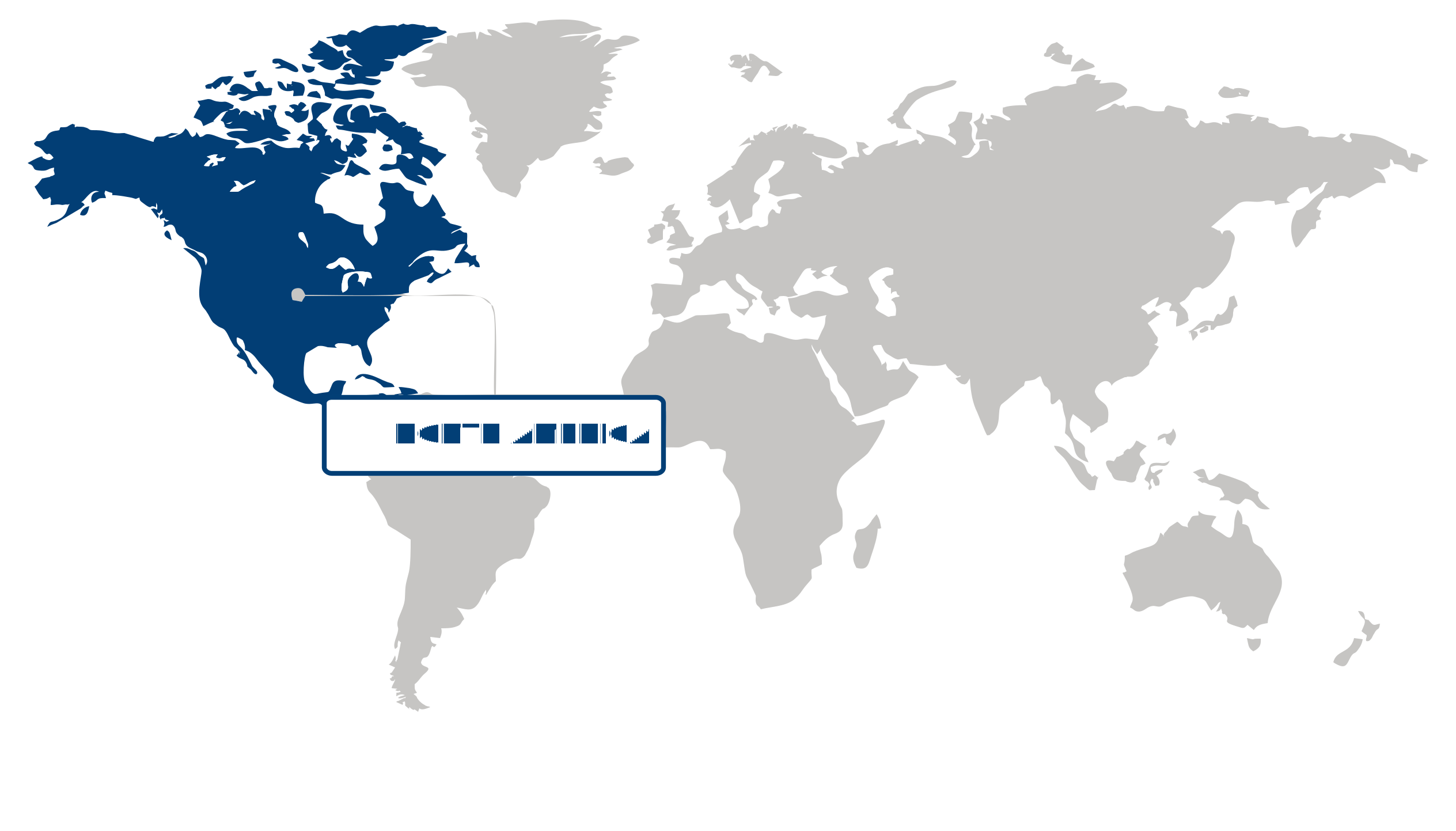
North America captured over 40.1% of the global nanofabrication market in 2025, the largest regional share, driven principally by sustained government R&D expenditure and rising demand for innovative nanotech solutions. Federal and national programs such as the National Nanotechnology Initiative, the U.S. National Science Foundation, the Department of Energy, and Canada’s Natural Sciences and Engineering Research Council have underpinned advanced materials and device research, while policy actions like the CHIPS and Science Act have accelerated translation into manufacturing; corporate investments from Intel, IBM Research, and Applied Materials further validate commercial momentum. Combined with resilient private-sector capital, deep talent pools, and integrated supply-chain capabilities, North America offers significant opportunities for scale-up in semiconductors, healthcare diagnostics, and energy applications.
The United States anchors the North American market, concentrating federal R&D and commercial scale-up that reinforce regional leadership in nanofabrication market. Agencies and programs—NIST, DARPA, NIH, the CHIPS and Science Act, and NSF-funded university centers at MIT, Stanford, and UC Berkeley—create a pipeline from discovery to deployment, while firms such as Intel, IBM Research, and Applied Materials convert research into toolsets and fabs. This combination of targeted public funding, university-industry collaboration, and corporate capex lowers commercialization risk and attracts specialist talent, making the U.S. the primary staging ground for regional growth and investor opportunity in nanofabrication.
Asia Pacific Market Analysis:
nanofabrication market in Asia Pacific emerged as the fastest-growing region, posting a robust CAGR of 20.16%, driven principally by the massive demand for consumer electronics and flat panel displays in China. This surge is reflected in capacity expansions by display manufacturers such as BOE Technology Group and TCL CSOT and reinforced by industrial policy signals from the Ministry of Industry and Information Technology (MIIT). Consolidated supply chains across China, Japan and Korea enable rapid scale-up, while advanced equipment vendors and precision materials suppliers strengthen regional capabilities. Talent concentration, digitalized process controls, and rising sustainability expectations further shape investment priorities. Together these dynamics make Asia Pacific the strategic focal point for investors targeting volume-driven, technology-intensive nanofabrication opportunities.
nanofabrication market Japan acts as the region’s high-value equipment and process-innovation hub, supplying advanced lithography, deposition and inspection tools used across Asia. Companies such as Tokyo Electron Limited and Nikon Corporation sustain high-margin technology cycles and collaborate with institutions including the Ministry of Economy, Trade and Industry (METI) and the National Institute of Advanced Industrial Science and Technology (AIST) to commercialize next-generation process modules. Japan’s supplier-led model mitigates regional bottlenecks and supports premium segments—serving as a key partner to Chinese and other APAC manufacturers. Strategically, Japan’s precision ecosystem increases the region’s resilience and accelerates adoption of complex nanofabrication technologies.
nanofabrication market China is the demand engine where massive consumer electronics and flat panel display consumption translates directly into wafer‑level and mask‑level scaling needs. Major OEMs and panel makers such as BOE Technology Group and TCL CSOT, alongside large consumer brands, drive predictable capital expenditure and rapid fab throughput requirements. Policy support from the MIIT and local provincial authorities lowers barriers to expansion and channels skilled labor into manufacturing clusters. For investors and strategists, China’s volume-driven demand provides clear routes to scale, supplier partnerships, and cost-competitive manufacturing that reinforce Asia Pacific’s overall growth trajectory in nanofabrication.
Europe Market Trends:
Held a commanding share, the nanofabrication market in Europe benefits from concentrated R&D and manufacturing clusters, policy support, and integrated supply chains that together attract scale-up capital and skilled talent. Recent moves by the European Commission (EU Chips Act) and Horizon Europe funding, together with financing mechanisms from the European Investment Bank, illustrate policy-led demand and capacity building; equipment and ecosystem leadership is visible through firms such as ASML and research collaborations with imec and the Fraunhofer Society. These signals—public grants, cross-border supplier networks, and localized advanced-manufacturing hubs—create sustained commercial opportunities for investors seeking resilient, innovation-led deployments across Europe. Europe’s combination of policy momentum and industrial depth points to continued strategic openings for scale and specialization.
Germany anchors the nanofabrication market as a manufacturing and systems-integration leader, leveraging strong applied research and industrial OEM partnerships. German strengths are evidenced by Fraunhofer Society applied-research programs and targeted support from the Federal Ministry of Education and Research (BMBF), alongside major industrial players such as Infineon and Bosch that maintain advanced fabrication and packaging capabilities. This operational depth—from prototype to production—lowers deployment risk for capital-intensive projects and positions Germany to absorb near-term demand for automotive sensors, power devices, and advanced packaging, reinforcing Europe-wide supply security and downstream scale opportunities.
France positions the nanofabrication market as an innovation-driven center focused on materials, device prototyping, and pilot-line commercialization. The CEA-Leti national lab and companies such as Soitec and STMicroelectronics, together with financing and innovation programs from Bpifrance, demonstrate a pipeline from materials R&D to early manufacturing. That combination promotes rapid translation of novel materials and process flows into pilot production, making France a strategic node for specialty substrates, MEMS, and photonics—capabilities that complement Germany’s scale and amplify regional value chains for investors and strategic partners.
| Parameter | North America | Asia Pacific | Europe | Latin America | MEA |
|---|---|---|---|---|---|
| Innovation Hub i Scale Nascent Developing Advanced | |||||
| Cost-Sensitive Region i Scale Low Medium High | |||||
| Regulatory Environment i Scale Restrictive Neutral Supportive | |||||
| Demand Drivers i Scale Weak Moderate Strong | |||||
| Development Stage i Scale Emerging Developing Developed | |||||
| Adoption Rate i Scale Low Medium High | |||||
| New Entrants / Startups i Scale Sparse Moderate Dense | |||||
| Macro Indicators i Scale Weak Stable Strong |
Segment Leadership and Growth Trends
Nanofabrication Market Share (%), Application, 2025
Go beyond the chart, access full insights & data tables
Request Free Sample ReportPharmaceutical represented largest share of the nanofabrication market in 2025. Leadership is rooted in extensive adoption of nanoscale fabrication for targeted drug delivery and precision formulation—directly reflecting the growth driver of increased use in pharmaceutical research and drug delivery systems. Demand for more effective biologics and patient-preferred targeted therapies, coupled with scalable nano-manufacturing investments and evolving regulatory pathways, has driven uptake; examples include Moderna’s lipid nanoparticle platforms and ongoing reviews by the U.S. Food and Drug Administration (FDA) that signal translational readiness. This position creates strategic openings for contract manufacturers, specialized equipment suppliers, and agile entrants offering analytics and process control, and continued material advances and digital process integration suggest the segment will remain central to therapeutic innovation in the near to medium term.
| Segment | Sub-Segment | Largest Segment | Fastest Growing |
|---|---|---|---|
| Application | Medicine, Pharmaceutical, Molecular Biotechnology, Cell Biology |
Competitive Landscape and Market Positioning
The competitive environment reflects concentrated capability-building and ecosystem alignment: coordinated initiatives to bundle lithography, deposition and inspection capabilities; selective consolidation to broaden service scopes; intensified engineering commitments to push resolution and throughput; and successive solution rollouts targeting advanced packaging and compound-semiconductor segments. These moves deepen account ties, raise interoperability requirements, and shift emphasis toward integrated, analytics-enabled toolchains that favor providers able to co-develop with leading fabs and design houses.
Strategic / Actionable Recommendations for Regional Players
Leverage proximity to cloud-scale customers and leading IDMs by strengthening co-development with system integrators and design teams, expanding AI-enabled metrology capabilities, and prioritizing advanced packaging and heterogeneous-integration offerings to capture adjacent value.
Build closer links with regional foundries and substrate suppliers through joint engineering centers, accelerate localized product adaptation for high-volume nodes, and align supply-chain partnerships to support compound-semiconductor and mobile-focused manufacturing ramps.
Differentiate via precision instrumentation and sustainability-driven process control by deepening collaborations with research institutes, tailoring tools for automotive and industrial segments, and emphasizing niche capabilities for quantum and specialty-device fabrication.
| Company | Market Share | Company Revenue | Revenue CAGR (%) | Product Portfolio | Geographic Presence | Innovation / R&D Focus | Strategic Developments |
|---|---|---|---|---|---|---|---|
| No companies available. | |||||||
Industry Development/News
| Company Name | Date | Key Development |
|---|
Explore This Report
Click a section of the wheel — or its numbered marker — to preview the custom segmentation, custom table of contents, or related reports available for this market.
Nanofabrication Market — Custom Segments
| Segment | Sub-Segment |
|---|---|
| No segment data available. | |
Nanofabrication Market — report.custom
| Custom Chapter | Custom Details | ||
|---|---|---|---|
| No custom TOC data available. | |||
Need a different cut of the data?
Request Custom ResearchWhat is the market size of nanofabrication?
What is the expected industry size of nanofabrication by 2035?
Which geographical area accounts for the highest portion of the nanofabrication market?
Which region shows the most rapid acceleration in the nanofabrication sector?
Which is the largest sub-segment within the application segment for nanofabrication industry?
Which organizations are considered leaders in the nanofabrication landscape?
Our Clients
"The reports offered a comprehensive view of the Food and Beverage landscape, covering market trends, consumer behavior, and competitive dynamics."
"Our experience in acquiring market research reports has been outstanding — the depth of analysis and actionable insights have proven invaluable."
"Fundamental Business Insights demonstrated a keen understanding of our business needs, delivering reports tailored to our specific objectives."
Our Research Team & Methodology
Every Fundamental Business Insights report is built by a dedicated vertical research team, validated through a structured primary-and-secondary methodology, and reviewed for accuracy before it reaches you.
Research Team Overview
Prepared by the Electronics & Semiconductors Research Team
Delivery
Published
Demand
Available
Support
Trust & Compliance
Research Domains
10 coverage areasResearch Intelligence
| Source Category | Research Sources | Purpose |
|---|---|---|
| Government Publications | Government agencies, statistical departments, regulatory bodies | Industry statistics, regulatory insights, and policy analysis |
| Company Disclosures | Annual reports, investor presentations, financial filings | Company performance, business strategy, and market positioning |
| Trade Associations | Industry associations and professional organizations | Industry developments, standards, and market perspectives |
| Technical Literature | Research papers, technical publications, academic journals | Technology developments and technical validation |
| Patent Analysis | Patent databases and intellectual property publications | Innovation trends, technology activity, and competitive research |
| Industry Databases | Established research databases and market intelligence resources | Market benchmarking, historical data, and industry analysis |
Research Workflow & Quality Assurance
Data Collection
Verified information gathered through primary and secondary research.
Data Triangulation
Cross-validation using multiple independent data sources.
Forecast Modelling
Market estimates developed using historical trends and analytical models.
Analyst Validation
Findings reviewed by domain experts for accuracy and consistency.
Editorial & Quality Review
Final editorial, quality, and compliance checks before publication.
Final Publication
Released after successful completion of the internal review process.
Report Coverage
📊 Market Assessment
- Market Size & Forecast
- Market Segmentation
- Regional Analysis
- Growth Drivers & Challenges
- Market Dynamics
🏢 Competitive Intelligence
- Competitive Landscape
- Company Profiles
- Competitive Benchmarking
- Mergers & Acquisitions
- Market Share Analysis or Key Company Strategies
🔍 Strategic Analysis
- Value Chain Analysis
- Porter's Five Forces
- PESTLE Analysis
- Pricing Trends
- Supply-Demand Analysis
🚀 Future Outlook
- Technology Landscape
- Regulatory Landscape
- Investment & Funding Landscape
- Emerging Opportunities
- Future Market Outlook
Have a question about this report or need a custom scope?
Request Customization